Zoom to microworld - Materials
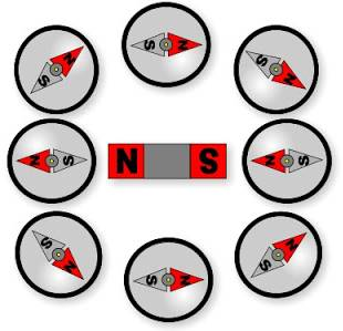
Needles
Img src
The earliest magnetic material known to man is magnetite, a naturally occurring magnetic ferrite. Pieces of this mineral were found to exert attractive or repulsive forces when brought close to another piece of the same material. Later, when iron objects became available, they were attracted to these earlier magnetic materials. When iron needles were rubbed against the magnetite, the needles also became imbued with this new bipolar property, giving the same attraction or repulsion as the original magnetite pieces. The subject of frictional magnetism may be one of the oldest questions about magnetism and still remains one of the least understood phenomena. These magnetized needles served as the first applications of magnetic materials since they functioned as compasses and allowed mariners to find North without the use of the stars.
The real beginning of modern magnetism as we know it today began in 1819 when Hans Oersted discovered that a compass needle was deflected perpendicular to a current bearing wire when the two were placed close to one another. It was at this point that electromagnetism was born. Next, Michael Faraday (1791-1867) discovered the opposite effect, namely that an electric voltage can be produced when a conducting wire cut a magnetic field.
Needlelike particles of a-Fe2O3 without micropores were attained by Kiyama (1992) by autoclaving in NaOH solution. Polyhedra-shaped magnetite for magnetic toner applications was made by Koma (1992) by precipitating ferrous hydroxide from ferrous chloride and sodium hydroxide in nitrogen. Bagul (1992) prepared active strontium ferrite powders by coprecipitation. The nitrate solutions of the metals were precipitated with sodium hydroxide and sodium carbonate. Submicron sized particles were formed.
Article src: Handbook of modern ferromagnetic materials, A. Goldman, B.S., Springer Science+Business Media New York, Ferrite Technology Worldwide, (1st edition), 1999.
Thin films
Img src
Much of the early research on magnetic thin films was done because of their prospective application as memory elements in digital computers. This application was never commercially successful, but was followed by the intense development of bubble domain memories, which also required the use of patterned magnetic thin films to control the motion of the bubbles. This development, too, eventually came to naught. But a rich variety of other uses, mainly related to various aspects of computer technology, have arisen. These include the original idea of magnetic memory, although in a somewhat different form from the earlier ideas.
A typical example of magnetic thin film, deals with the widely used alloy called 80 permalloy (80 wt% Ni, 20% Fe), which has low anisotropy and low magnetostriction combined with reasonably high magnetization, and is easily made in thin-film form. It is the obvious choice when a soft magnetic thin film is required.
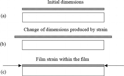
Thin films are made by depositing atoms onto a substrate, and are almost always measured and used while bonded to the substrate. Interactions between the substrate and the film are therefore important, and the surface condition and temperature of the substrate during the deposition of the film are variables to be controlled. Thin films may be made in a variety of ways: chemical vapor deposition, electrodeposition from a liquid electrolyte, thermal evaporation (using one of several different heat sources), and sputtering. Of these, sputtering is the most widely used, mostly because it permits almost any combination of elements to be deposited. Sputtering is a physical rather than a chemical or thermal process. Atoms are physically ejected from a target material by high-energy gas ions, usually argon. It is necessary to create a plasma of ionized gas in the deposition chamber. The presence of this plasma, and the gas atoms needed to create it, means that the deposition conditions are much less pure than in the case of thermal evaporation, which can be carried out under very high vacuum conditions. Despite these difficulties, thin film production by sputtering can be done in a highly reproducible way, and sputtering is used, for example, in the production of the various layers on the disk surface of hard disk drives.
Article src: Introduction to Magnetic Materials (2nd Edition), B. D. Cullity, C. D. Graham, Wiley-IEEE Press, 2008.
Wires
Img src
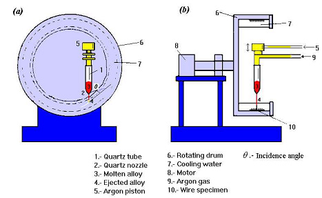
These consist of structures where the length is much larger than the width, and therefore the relevant geometrical parameters are the width and thickness. A large body of work has been devoted to the study of wire structures and a number of fabrication techniques have allowed the fabrication of magnetic wires with widths ranging from a few nanometers to several micrometers. Depending on the fabrication process, planar wires, or wires with circular cross section can be fabricated (namely, by electrodeposition using porous membranes as templates).
Amorphous wires prepared by the in-water-quenching technique exhibit a bistable magnetic behavior, regardless of the sign of magnetostriction. This property derives from the special domain structure that is formed in the wire, typically made of an active longitudinal core, reversing its magnetization with a single Barkhausen jump, and an outer shell, having either radial or circumferential domains.
The origin of such a structure is to be found in the anisotropies induced by the large stresses frozen-in during the solidification process, in association with the anisotropy of magnetostatic origin (shape anisotropy). The switching-like behavior of the magnetization reversal in amorphous wires can be exploited in a number of applications, such as jitter-free pulse generators, digitizing tablets, speed and position sensors, and antitheft devices. A further remarkable property of amorphous wires is that their reactance at MHz frequencies can change to a large extent upon application of a DC field (giant magnetoimpedance effect).
Article src: Handbook of Magnetism and Advanced Magnetic Materials, H. KronmÜller and S. Parkin, Volume 1: Fundamentals and Theory, John Wiley & Sons, 2007.
Article src: Measurement and Characterization of Magnetic Materials, F. Fiorillo, Istituto Elettrotecnico Nazionale Galileo Ferraris, Torino, ITALY, Elsevier Series in Electromagnetism, 2004.
Multilayer microwires
Img src
Owing to the cylindrical symmetry, the preparation of multilayered microwires by adding external layers or microtubes to existing wires has been studied. First, attempts were reported in Rauscher and Radeloff (1991) where composite microwires were prepared consisting of a soft NiFe-based core and a hard CrCoFe shell. There, the magnetic interactions between components play an important role to determine the bistable magnetic behavior of the core.
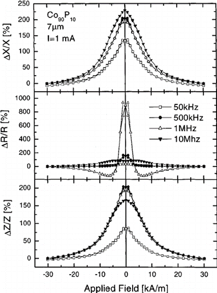
Attempts were performed by electrochemical deposition of CoP, CoFeNi, and CoNi alloys onto Cu-rich microwires which was used as electrode. The objectives for fabrication of these microtubes onto metallic nonmagnetic microwires were related to their magnetoimpedance properties. Owing to the differential conductivity and especially their permeability, the magnetoimpedance behavior was expected to show a particular response. In fact, quite large variations of the imaginary component of impedance were reported.
Additionally, interest lies in the preparation technique itself that allowed the fabrication of novel materials with nonstandard properties. Electrodeposition of outer layers to microwires opens new possibilities for controlled behavior such as modifiable easy magnetization axis (from radial to in plane of the layer) depending on thickness and electroplating parameters. Figure shows the domain structure at the surface of a Co microlayer onto Cu microwire where the existence of radial anisotropy is deduced.
Article src: Handbook of Magnetism and Advanced Magnetic Materials, H. KronmÜller and S. Parkin, Volume 1: Fundamentals and Theory, John Wiley & Sons, 2007.
Magnetic microparticles

Img src
Small ferrimagnetic particles appear naturally in igneous rocks, and ferromagnetic and ferrimagnetic particles can be synthesized by a variety of chemical methods. The smallest magnetic particles exhibit superparamagnetism, behaving like paramagnetic macrospins. Larger ones adopt magnetic configurations which are governed by the balance of anisotropy, exchange and magnetic dipole interactions. Submicrometre spots of magnetic materials can be patterned from thin films. When magnetocrystalline anisotropy is negligible, the small elements tend to adopt configurations where the magnetization is oriented as far as possible parallel to the surface. They can do this because the exchange length, which is the length scale over which the direction of magnetization of a ferromagnet can adapt to dipolar fields, is only 2–5 nanometres.
Surface anisotropy can also influence the magnetic configurations of ferromagnetic nanoparticles, when the exchange is not too strong. Some examples are shown in figure. These effects are unimportant in nanoparticles of 3d metals and alloys with Curie points above room temperature, but they may be significant for rare-earth alloys with low Curie points, or actinide ferromagnets like US, where the single-ion anisotropy is exceptionally strong.
However, magnetic methods are beginning to make a contribution to the study of cells, and subcellular structures such as proteins and biomolecules. Generally, these studies make use of magnetic microparticles whose sizes are compatible with the sizes of the biological structures they are used to manipulate (10–100 μm for cells, 10–100 nm for proteins). The microparticles normally incorporate many superparamagnetic nanoparticles in a biocompatible polymer microbead, with a fill fraction 0.1 < f < 0.8.
Article src: Magnetism and Magnetic Materials, J. M. D Coey, Cambridge University Press, 2010.
Organic semiconductors
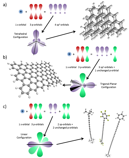
Schematics of the electronic orbitals of a) sp3 hybridisation (diamond), b) sp2 hybridisation (graphene) and c) sp hybridisation (heptayne, octayne and dodecayne linear acetylenic carbon, with various capping groups).
Img src
Organic semiconductors are very promising materials for spin valves, and therefore for GMR read heads. This is because of the large spin relaxation time in conjugated molecules, but also due to rather simple and low energy consuming device fabrication techniques. However, a big challenge facing organic spin valves at the moment is the necessity for low-temperature operation in most studied cases, which does not make them competitive in the magnetic recording industry. Nevertheless, we are witnessing ever increasing developments in their material properties and there is hope that more of these organic spin valves will be capable of room temperature functionality in the near future. Most studies of spin injection into organic semiconductors focus on the organic material known as Alq3, or tris (8-hydroxyquinoline) aluminum. It would be interesting to have a look at other candidates, such as the perylene derivative PTCTE, or tetraethyl perylene 3,4,9,10- tetracarboxylate. Charge mobilities in organic materials are orders of magnitude smaller than in semiconductors; however, electron mobility in both Alq3and PTCTE is about the same order of magnitude. The newly acquired popularity of PTCTE as spin valve contenders is due to the fact that perylene molecules were used as electron transport materials in optoelectronic devices like organic electroluminescent diodes (OLEDs) and solar cells. When placed between ferromagnetic materials such as NiFe and Co, PTCTE spacer layers of 300 nm lead to overall GMR responses of up to 3%. Assuming an exponential decay of spin polarization, this GMR values corresponds to 100–150 nm spin diffusion length which is a high reported value.
Article src: Magnetism: Basics and Applications, Stefanita, Carmen-Gabriela, Springer Heidelberg Dordrecht London New York, 2012.