Down to nanoscale - Materials
Magnetic nanostructures

Img src
Nanostructured materials have large surface area to volume ratios, which can result in inhomogeneous magnetic properties. Due to the quenching of orbital moments in the bulk, there is no orbital contribution to total magnetic moment; hence, magnetic moment in the bulk is generally lower than that at the surface.
Img src
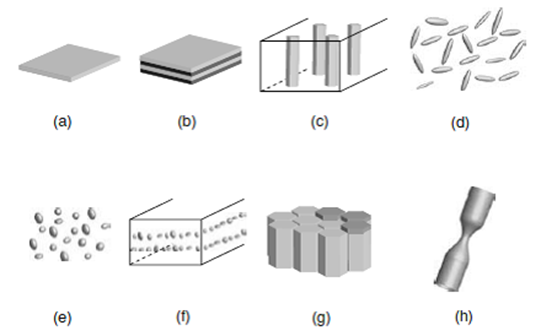
Examples of magnetic nanostructures: one small dimension: (a) thin film and (b) multilayer stack; two small dimensions: (c) nanowire array and (d) acicular particles; three small dimensions: (e) nanoparticles, (f) nanocomposite, (g) thin-film recording medium and (h) nanoconstriction
The wide range of chemical compositions as well as wide variety of nanostructures requires a variety of processing techniques, each technique being restricted to a relatively narrow class of magnetic materials; For example, nanostructured magnetic powders are produced by ball milling, anisotropic/isotropic magnetic ribbons are prepared by melt spinning, nanostructured thin films of both hard and soft magnetic materials are produced by sputtering, molecular beam epitaxy, and electrodeposition.
Article src: Handbook of Nanomaterials, R. Vajtai, Springer-Verlag Berlin Heidelberg, 2013.
Magnetic multilayers
Img src
Study of magnetic thin films provides understanding of magnetic properties of nanostructured materials in 2-D systems. The magnetic characteristic length is dependent on the dimensionality as well as on the surface/interface electronic structure, due to which interesting effects are observed. Examples are moment enhancement, surface anisotropy, change in Curie temperature, and thickness-dependent domain wall formation.
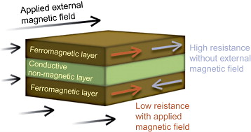
Thin-film or multilayer magnetic nanostructures have only one dimension in the nanoscale range. Magnetic and nonmagnetic layers are stacked to make heterostructured thin films, which have applications in spin valves, tunnel junctions, GMR, etc. Magnetic thin films show interesting magnetic phenomena such as perpendicular anisotropy, moment modifications at surfaces and interfaces, and thickness-dependent domain wall motion.
Magnetic thin films are of considerable interest; sputtering, molecular beam epitaxy, and electrodeposition are some of the techniques used for thin-film magnetic nanostructure development.
Magnetic multilayers are formed of alternating layers of magnetic and nonmagnetic metal. When the layers are all epitaxial, the multilayer becomes a superlattice. Heterostructures can also be made of magnetic layers in direct contact one with another; there will be direct exchange coupling at the interface.
Indirect exchange coupling in multilayers is mediated by spin polarization in the nonmagnetic layers, provided they are thin enough. Dipolar interactions also play a role in coupling ferromagnetic thin films. For alloys and multilayers, multiple sources with individual power supplies are required. The source–substrate distance is usually at least 300 mm.
New playing ground is opened by nanoscale multilayer interfaces of correlated materials. Careful control of orbital structure at interfaces between two materials can generate novel physical phenomena and functionalities, that are not a property of the constituent materials themselves. Examples are bilayers of Mott and band-insulating materials yielding a metallic interface. Other possibilities are combination of CMR manganite and high-TC superconducting materials.
Article src: Magnetism and Magnetic Materials, J. M. D Coey, Cambridge University Press, 2010.
Article src: Handbook of Nanomaterials, R. Vajtai, Springer-Verlag Berlin Heidelberg, 2013.
Article src: Handbook of Magnetism and Advanced Magnetic Materials, H. KronmÜller and S. Parkin, Volume 1: Fundamentals and Theory, John Wiley & Sons, 2007.
Magnetic monolayers

Img src
Magnetic films with thicknesses ranging from a single monolayer to upwards of 100 nm may be grown on crystalline or amorphous substrates by a variety of physical or chemical methods. An epitaxial single crystal film is one that grows in perfect atomic register with a single-crystal substrate. An oriented film has one specific crystal axis oriented perpendicular to the substrate. The region of the film near the interface may be highly strained if there is a difference in lattice parameters between film and substrate. The compressive or expansive biaxial strain is accompanied by a strain of opposite sign in the direction normal to the substrate. Excess strain is relaxed in thicker films by atomic-scale dislocations as the film eventually adopts its equilibrium lattice parameters far from the substrate. When the lattice mismatch is too great (>4%), or if the substrate is amorphous (e.g. glass) it has less ability to dictate the structure of the film growing on it. Substrates can be chosen to influence the crystallographic or magnetic texture of the film directly, or else a thin seed layer can be deposited first to do the job.
Dramatic modifications of magnetization are found in films a few monolayers thick. Vanadium and rhodium become ferromagnetic in films 1–2 monolayer thick, although they are nonmagnetic in bulk. Metals such as palladium which have an enhanced paramagnetic susceptibility, become ferromagnetic when deposited on a substrate of iron or nickel. The example of nickel on copper is illustrated in figure.
The magnetic properties of iron are notoriously structure-sensitive. While the bcc form is ferromagnetic, fcc iron may be nonmagnetic, antiferromagnetic or ferromagnetic, depending on the lattice parameter. When grown epitaxially on fcc copper, the magnetic properties of an iron film depend on the substrate temperature during deposition. Ambient temperature gives ferromagnetic fcc iron films, but when the substrate is cooled, they are antiferromagnetic.
Article src: Magnetism and Magnetic Materials, J. M. D Coey, Cambridge University Press, 2010.
Magnetic nanowires
Img src
Interesting spintronic chips with racetrack memory made of magnetic domains within nanowires have become nowadays one of the latest storage devices to be comprehensively investigated. Nanowires lie horizontally or stand vertically on silicon substrates while magnetic domains contained in the nanowires store bits of data. The domains are moved rapidly along the tracks by pulses of electric current. Magnetic fields emanating from the domain wall set the magnetization direction in the racetrack’s bit. Thus, the domain wall separating two oppositely magnetized domains is used to write a data bit on the racetrack. While the magnetic domains pass a sensor lying underneath the nanowire, the changing magnetization between oppositely magnetized domains is recorded.
Because of this rapid displacement along the track past read/write heads placed at fixed locations, these information storing magnetic nanowires are known as “racetrack memory.” The magnetic domains are nonvolatile and rewritable, thereby comparable to HDD. Nevertheless, one of their big advantage over HDD is that the chip has no mechanical moving parts because only electrons read and write bits. This also makes them very fast, while not compromising on reliability.
Each magnetic domain represents a “1” or a “0” of stored data, and retains its data when power is switched off. The sensing layer of the magnetic head changes its magnetization back and forth in order to match the field of each domain passing it. Domain walls can move as fast as 150 nm/ns, allowing access millions of times faster than HDDs. With perpendicular columns of nanowires, large data densities become possible on one silicon chip, overcoming many limitations of their predecessor memories. As bits move rapidly along the racetrack, a new generation of data intensive applications is envisaged, especially since the magnetic heads themselves have evolved. From the spin valve sensors relying on GMR (Giant Magnetoresistance) to the MTJs (Magnetic Tunnel Junctions) exploiting TMR (Tunneling Magnetoresistance) to achieve a greater sensitivity to small magnetic fields, new spintronic technologies come to the aid of magnetic recording. As such, the racetrack memories benefit from spintronics as well.
Article src: Magnetism: Basics and Applications, Stefanita, Carmen-Gabriela, Springer Heidelberg Dordrecht London New York, 2012.
Magnetic Nanorings
Img src
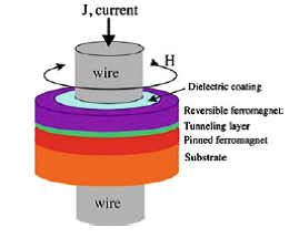
In nanoring designs, the bit can be encoded by the direction of the vortex magnetization state in the ferromagnetic thin film ring. However, even this mechanism has its difficulties given that it requires creating magnetization poles at the boundaries of the ring, thus needing elaborate writing schemes, or even very high current densities able to switch the magnetization state. What makes the design and operating principle of the device represented in figure more likely to succeed is that it uses the polarity of strictly localized 360o domain walls in the free ferromagnetic layer to encode the bit of information. The existence of these types of domain walls has been previously predicted by several simulations. In the presence of a 360o wall, the magnetization looks like a vortex state in most of the ring, except in that specific area where the ring is localized. However, it is not quite a typical vortex, since inside the wall the magnetization rotates in plane, in the direction opposite to the direction of rotation in the rest of the ring. Therefore, both states representing ±360o walls can be attained by a simple in plane rotation of the magnetization vector, avoiding any out of plane complications. As such, the current carried by the wire passing through the ring configuration and generating a circular magnetic field is capable of easily switching between the two polarities of the 360o wall. At the same time, readout can occur because the nanorings are part of a magnetic tunnel junction configuration.
Article src: Magnetism: Basics and Applications, Stefanita, Carmen-Gabriela, Springer Heidelberg Dordrecht London New York, 2012.
Magnetic Nanodots

Img src
The morphology of the hcp nanodots is easily understood: the hcp nanodots are the same truncated hexagonal bipyramids shown in figure, whose axis coincides with the c-axis of the hcp lattice. These bipyramids are cut to expose (0001), (1011), and small (1120) surfaces. A larger (1120) face is in contact with the substrate, where Ni atoms assume a typical configuration in zigzag rows. The driving forces leading to the stabilization of the hcp nanodots can be extended to other metal/oxide couples: Pd/CaO, Pt/CaO, Ni/CoO, and Co/MgO. It is to be noted that Ni, Pd, and Pt are fcc rather than hcp in the bulk, so that a transition to fcc configurations is expected to occur with increasing size of the particles. In fact, experiments on Ni particles on MgO (100) observe the hcp morphology at small sizes and locate a transition to the usual fcc (001) structures for diameters larger than about 5 nm. At the theoretical level, the comparison of hcp and fcc (001) motifs as a function of size locates this transition between 2000 and 2500 atoms, corresponding to cluster diameters of about 4.5 nm, in excellent agreement with experimental data.
Furthermore, nanodots may offer additional improvements in device performance due to their strict electron confinement. It is believed that if the position of each electron is fixed by confining it in a restricted region such as a “dot,” the energy distribution in that region will not experience large temperature variations. Each region could be a nano- or a quantum dot that effectively prevents the electrons from being thermally excited to higher energy states.
Article src: Handbook of Nanomaterials, R. Vajtai, Springer-Verlag Berlin Heidelberg, 2013.
Article src: Magnetism: Basics and Applications, Stefanita, Carmen-Gabriela, Springer Heidelberg Dordrecht London New York, 2012.
Ferrofluids

Img src
A ferrofluid resembles a ferromagnetic liquid, but it is really a colloidal suspension of tiny superparamagnetic particles in oil or water. Chemical techniques were developed in the 1960s to disperse nanoparticles of magnetite or maghemite 3–15 nm in diameter in such a way that they do not agglomerate into chains under the influence of dipole–dipole interactions, when subject to an external magnetic field. In order to stabilize the colloid, it is necessary to weaken the dipole–dipole forces, which fall off as r −3. Ways to keep the particles apart are to coat or embed each particle in polymer. A sheath of surfactant molecules on the surface of the oxide particles helps make them soluble in water. Otherwise charged nanoparticles can be dispersed in an ionic liquid.
Each particle has a thermal energy of order kBT , or 4 × 10⁻²¹ J at room temperature. Besides the Néel-type superparamagnetic relaxation, the particles are subject to normal Brownian motion, which helps to stabilize the colloid. A stable ferrofluid should be impervious to sedimentation under the influence of gravity, and it should neither drift in a magnetic field gradient nor agglomerate under the influence of dipole forces. These requirements impose a particle size of order 10 nm. Particles this small are single-domain.
Magnetic nanoparticles make up a fraction f of the total volume of the ferrofluid, which is at most 20%. The magnetization of magnetite is 480 kAm−1, so the saturation magnetization of a commercial, magnetite-based ferrrofluid does not exceed 100 kAm−1. A typical value is 50 kAm−1. On account of their energy, size and separation, the particles behave like weakly interacting paramagnetic macrospins, each with a moment m ∼ 103–105μB.
Article src: Magnetism and Magnetic Materials, J. M. D Coey, Cambridge University Press, 2010.
Magnetic Nanoparticles

Img src
Numerous physical and chemical methods have been employed to produce magnetic nanoparticles. These include sputtering, metal evaporation, ball milling, electrodeposition and solution phase chemistry synthesis, among which the solution phase synthesis has been seen as the most promising approach for preparing monodisperse magnetic nanoparticles. It is known that solution phase chemistry can offer an important homogenous nucleation step and facilitates the controlled growth of the nuclei suspended in the solution. As a result, magnetic nanoparticles with various monodisperse sizes and shapes have been prepared. Furthermore, magnetic nanoparticles prepared in this solution phase chemistry can be readily stabilized against particle aggregation or oxidation with a layer of robust organic or inorganic coating. The stabilized nanoparticle dispersion can be deposited on a solid substrate and the solvent is allowed to evaporate. By controlling the concentration of the particle dispersion and the solvent evaporation rate, 2D or 3D self-assembled magnetic nanoparticle superlattices can be formed.
Three small dimensions define a nanoparticle. Again the magnetic particles may be separate and dispersed, or embedded in a medium to form some kind of composite. The materials in the bulk heterostructure may both be magnetic, or one magnetic and the other not. By suitable engineering of the nanocomposite, unique combinations of magnetic properties or magnetic and nonmagnetic properties may be achieved that are unattainable in any homogeneous bulk material. Magnetic nanoparticles can be structured in lines or planes. Examples of the latter are patterned thin films or multilayers, and granular magnetic recording media such as Co−Pt−Cr films.
Nanoparticles, which are not quite small enough to be thermally excited over the energy barrier, can nevertheless exhibit spontaneous coherent fluctuations of their magnetic moment around the energy mimimum. These excitations take the place of long-wavelength spin waves, which cannot be excited because the particle size fixes a maximum possible wavelength.
In the antiferromagnetic state, the magnetic moments of the individual atoms of the material have an antiparallel arrangement for a two‐dimensional system. In the antiferromagnetic state, the material has no net magnetic moment and the susceptibility will be zero. Antiferromagnetic nanoparticles display unusual behavior compared to ferromagnetic nanoparticles. In 1961, Néel proposed that antiferromagnetic nanoparticles could display weak ferromagnetism and superparamagnetism.
As the particle size decreases, the percentage of atoms on the surface of the particle increases. Néel proposed that for antiferromagnetic nanoparticles, the antiparallel orientation of the moments on the surface would be lost and that the moments of the surface atoms would actually align ferromagnetically parallel to the axis of the antiferromagnetic alignment in the interior of the particle. This idea means that an antiferromagnetic nanoparticle can be viewed as having an inner antiferromagnetic core surrounded by an outer shell of ferromagnetically ordered spins. Experimental measurements in nickel oxide (NiO) confirm this model. Bulk NiO has a rhombohedral crystal structure and becomes antiferromagnetic below 523 K. Above that temperature, it is paramagnetic and the crystal structure is cubic. Figure shows a measurement of the dc susceptibility of NiO nanoparticles versus temperature for particles of two different sizes, which were ZFC, and measured in a field of 100 G. The presence of a nonzero susceptibility means the antiferromagnetic particles are displaying ferromagnetic behavior.
For particles greater than 100 nm, the susceptibility is zero. For the smaller particles, the figure shows that the susceptibility increases with increasing temperature to a maximum and then decreases. The dc magnetic field at which the maximum occurs shifts to higher temperature as the particle size gets smaller, and the magnitude of the susceptibility increases with reduced particle size.
Article src: Handbook of Magnetism and Advanced Magnetic Materials, H. Kronmuller and S. Parkin. Volume 1: Fundamentals and Theory, John Wiley & Sons, 2007.
Article src: Physics of Magnetic Nanostructures, First Edition. Frank J. Owens, Inc. Published by John Wiley & Sons, Inc., 2015.
Molecular nanomagnets
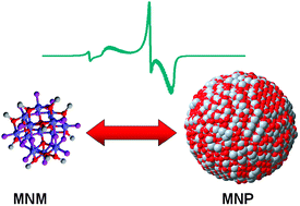
Img src
Another class of magnetic nanostructures are molecular nanomagnets, sometimes termed single-molecule magnets. Magnetic molecular clusters are intermediate between classical and quantum magnets and show unusual properties. Molecular nanomagnets are mainly organic molecules that are bonded to metals with unpaired electrons. Molecular nanomagnets are promising candidates for observations of quantum phenomena due to their well-defined structure and well characterized spin state. Thermally activated quantum tunneling of magnetization was first observed in molecular nanomagnets.
Article src: Handbook of Nanomaterials, R. Vajtai, Springer-Verlag Berlin Heidelberg, 2013.
Quantum dots

Img src
The ultimate ‘zero-dimensional’ magnetic nanostructure is a dot so small that it contains few electrons, or maybe even a single one. The capacitance of a sphere of radius r is C = 4πε0r. The potential of a single electron on the sphere is V = e/C; for example, if r = 14.4 nm, V = 100 mV. This Coulomb barrier to adding charge to the nanodot capacitor is known as Coulomb blockade. The electron content of the quantum dot can be controlled by tunelling electrons, one at a time, by adjusting the bias of the adjacent electrodes, which may be ferromagnetic.
The quantum dot is really an artificial atom, with a square-well potential rather than a Coulomb potential. At low temperature the unpaired spin moment of the dot can form a Kondo singlet state with electrons in nonmagnetic electrodes. Spin-polarized electron flow across it can be regulated by adjusting the potential of a gate. This is a magnetic single-electron transistor. Pairs of these magnetic quantum dots are candidate q-bits for a quantum computer.
Article src: Magnetism and Magnetic Materials, J. M. D Coey, Cambridge University Press, 2010.